Using Ansys SIwave 2020R2.
This post introduces a basic IR-drop analysis on the power planes using SIwave 2020R2.
- Analyze the voltage drop of one power rail, from source to chip.
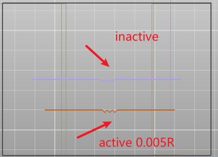
- All the RLC components are deactivated except for those connected in series to the power rails.
SIwave Documentation: Computing DC IR Simulations
New Project
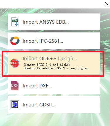
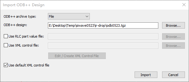
Import ODB++
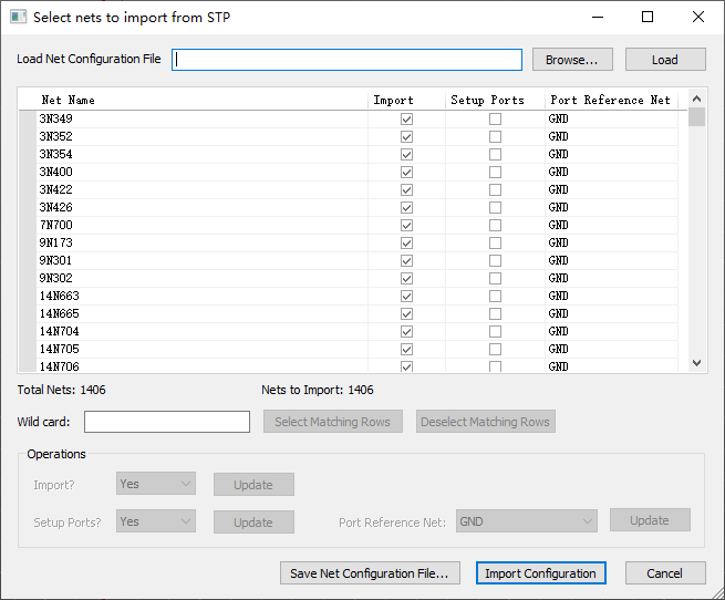
default setting for nets.
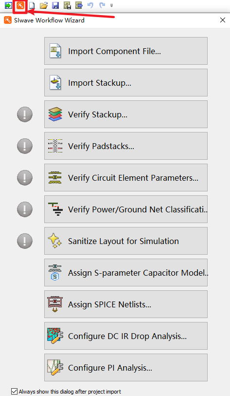
The Workflow Wizard
Open the Workflow Wizard from this button on the upper-left.
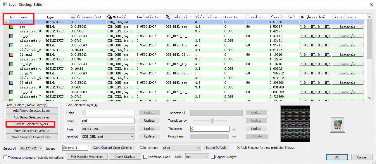
Stackup
Delete the smt layers above top and below bottom (they have 0 thickness and would cause simulation error).
(For IR-analysis, the dielectric material is not important, so use default.)
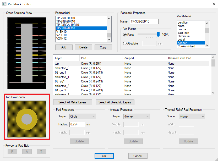
Padstack
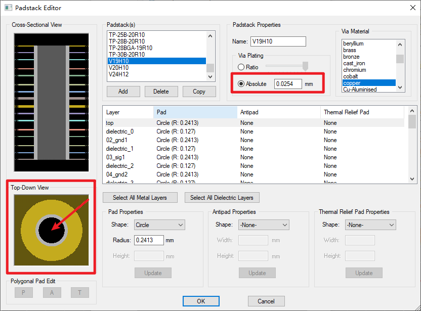
Mainly, the via plating setting. Default:
Change it to 1mil (or something else, according to the manufacturer).
Verify Circuit Element Parameters
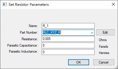
Deactivate all the RLC elements.
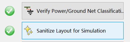
Power/Ground Net and Sanitize Layout
Default. Here are the documentations.
Identifying Power and Ground Nets
Sanitize Layout is an operation for cleaning power and ground nets in order to fix certain alignment problems as well as complexities that may slow down simulation. It works by uniting the planes and traces for each net to be cleaned. Once the united planes are formed, portions that display trace-like properties are converted into traces.
Connect the two planes
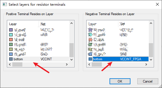
The VCCINT plane is smulated. The resistor in series is for current sensing, connecting the two planes, VCCINT and VCCINT_FPGA.
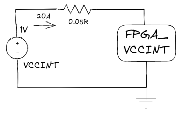
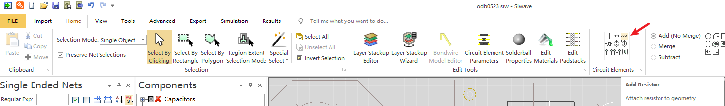
Add an ideal resistor to connect VCCINT and VCCINT_FPGA in the simulation.
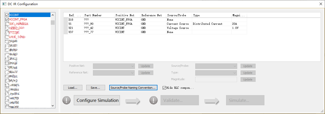
Configure DC-IR Drop
VCCINTandVCCINT_FPGAare both selected.- U21 is the power supply, set it as
voltage source. - U1 is the FPGA chip, set it as
current source(alsoDistributed Currentso that each power supply pin is simulated as a small load).
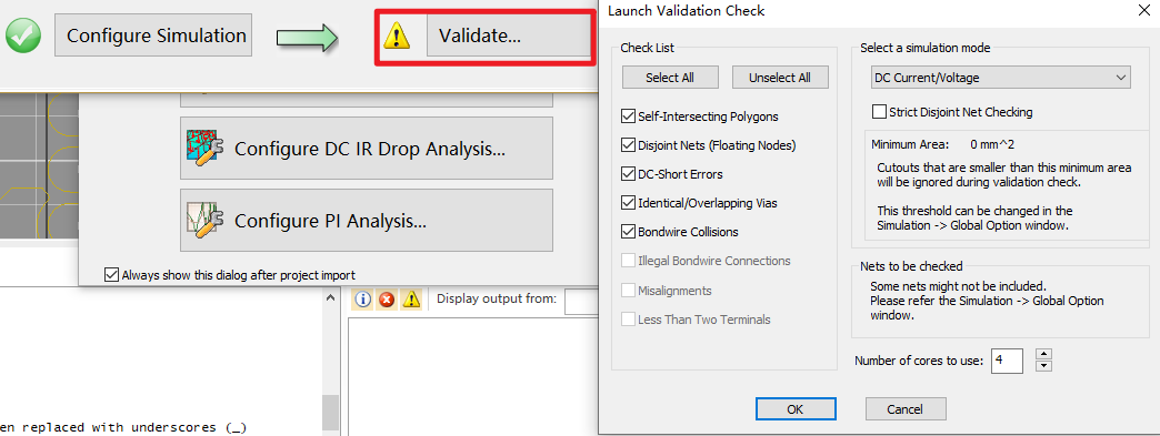
Follow Configure--Validate--Simulate to start IR simulation.
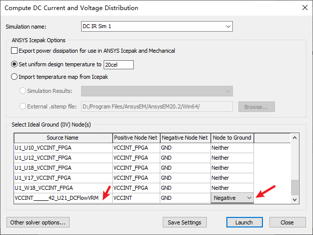
About Node to Ground
From documentation: mainly, select Negative for voltage source and Neither for everything else.
Use the Node to Ground drop-down menu to select Neither, Negative, or Positive.
- If you select Negative on a voltage source, the voltage display on its ground pin will be 0 V.
- If you select Positive on a voltage source, the voltage display on its ground pin will be negative. Consider this as being the 0 node in a SPICE simulation. This is the node to which you want all voltages referenced. Since SIwave includes the return paths of all planes (including the ground), we cannot assume that all of the sources reference that 0 node. Thus we have to pick one to be the absolute 0 node reference. So if we put the 0 node on the positive side of a voltage plane, the “ground” or return path would show as negative.
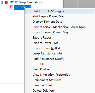
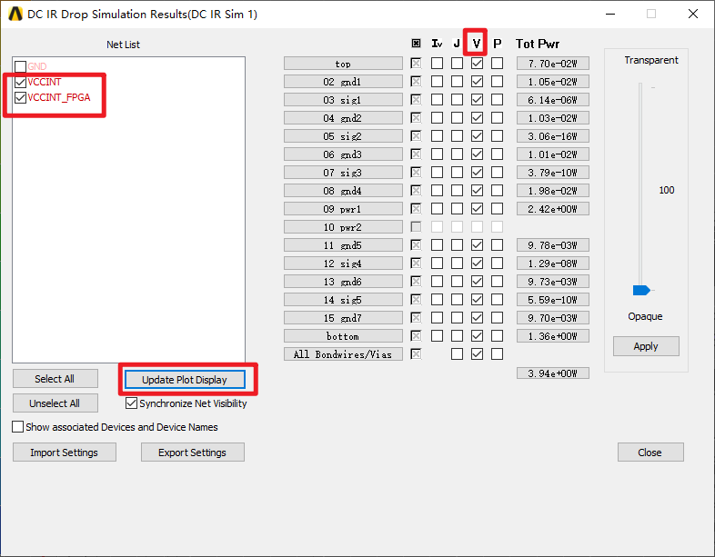
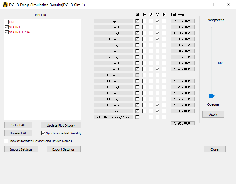
Displaying Results
Plot Current/Voltages
This example displays voltage level.
- Select certain layers for display
- Display other stuff such as current density (J) or power (P).
View-turn off Display Mesh, for a cleaner look.
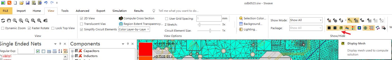
Display only layers 1,3,4,9,15,16:
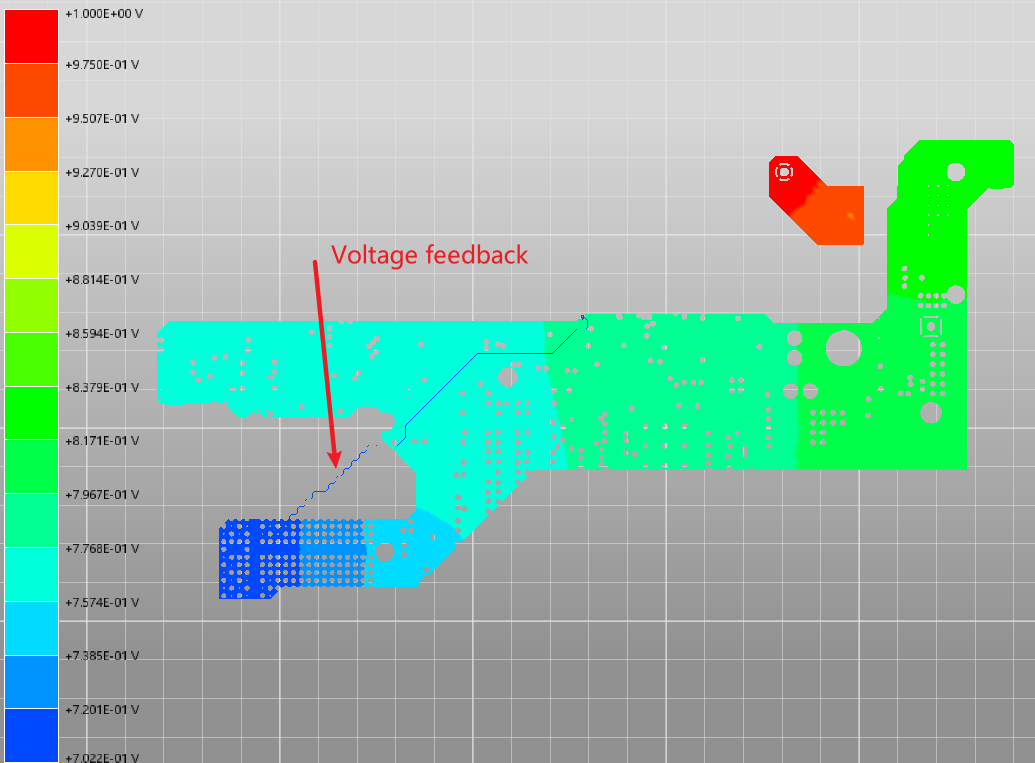
The results:
- The red one is
VCCINT, the source, at almost 1V - Between
VCCINTandVCCINT_FPGA(the green one), is the voltage drop on the current sensing resistor (0.005R*20A=0.1V) - The total voltage drop from source to load is around 0.3 V. But in reality, the voltage feedback trace will compensate for the voltage drop, so that the load voltage is 1V (and the source voltage is about 1.3V).